What opportunities and challenges are AI chip manufacturers facing under the background of big model?
Editor’s Note: This article comes from WeChat WeChat official account Rui Rui Insight (ID:siruidongcha) and is reproduced by Entrepreneurial State with authorization.
From ChatGPT on November 30th, 2022 to 360 Smart Brain Model 2.0 on June 13th, 2023, the global AI community has been crazy about the big model for more than seven months. ChatGPT have sprung up like mushrooms after rain, throwing "bombs" into the AI market: office, medical care, education, and manufacturing, which are in urgent need of AI empowerment.
And the AI application is tens of millions, and it is the last word to build a big model.
For the big model "world", the algorithm is "production relationship", which is the rule and way to deal with data information; Computing power is "productivity", which can improve the speed and scale of data processing and algorithm training; Data is "means of production", and high-quality data is the nutrient that drives the algorithm to iterate continuously. Among them, the calculation force is the premise to make the big model rotate.
As we all know, the big model is putting forward unprecedented requirements for computing power. The specific performance is as follows: According to NVIDIA data, before there is a big model based on Transformer model, the computing power demand is roughly increased by 8 times every two years; Since the use of the Transformer model, the demand for computing power has increased by 275 times every two years. Based on this, the Megatron-Turing NLG model with a parameter of 530B will consume more than 1 billion FLOPS of computing power.

(AI’s iteration of different model algorithms. Source: Gelonghui)
As the brain of the big model, AI chip is the basic premise to support the efficient production and application of ChatGPT. Ensuring efficient and sufficient supply of computing power is an urgent problem for AI chip manufacturers.
At the same time, GPT-4 and other big models have opened their mouths to chip manufacturers, which also brings good news to chip manufacturers, especially start-up chip manufacturers: the ecological importance of software is declining.
When the technology was not mature enough, researchers could only start from solving a specific problem, and a small model with less than one million parameters was born. For example, DeepMind, an AI company owned by Google, allows AlphaGO to "learn" the chess steps of millions of human professionals.
With more small models, the adaptation of hardware such as chips is imminent. Therefore, when NVIDIA introduced the unified ecological CUDA, GPU+CUDA quickly won the recognition of computer science and became the standard configuration of artificial intelligence development.
Nowadays, the emerging large models have multi-modal ability, which can deal with text, pictures, programming and other issues, and can also cover many vertical fields such as office, education and medical care. This means that adapting to the mainstream ecology is not the only choice: when the demand for chips for large models soars, chip manufacturers may be able to complete orders for multiple small models only by adapting to 1-2 large models.
In other words, the emergence of ChatGPT provides opportunities for start-up chip manufacturers to overtake in corners. This means that the market structure of AI chips will undergo great changes: it is no longer a one-man show of individual manufacturers, but a group show of many innovators.
This report will sort out the development situation of AI chip industry and players, sum up the path for players to improve their computing power in the era of big computing power, and based on this, spy on the development trend of AI big computing chips.
At present, AI chips are divided according to the types of technical architecture, mainly including GPGPU, FPGA, ASIC represented by VPU and TPU, and integrated memory and calculation chips.

According to its location in the network, AI chips can be divided into cloud AI chips, edge and terminal AI chips;
The cloud mainly deploys AI training chips and reasoning chips with high computing power to undertake training and reasoning tasks, such as intelligent data analysis and model training tasks.
Edge and terminal mainly deploy reasoning chips to undertake reasoning tasks, and need to independently complete data collection, environmental awareness, human-computer interaction and part of reasoning decision control tasks.

According to its practical goal, it can be divided into training chip and reasoning chip:

Throughout the development history of AI chips in China, the localization process of AI chips can be roughly divided into three eras.
Since the internet wave kicked off the AI chip in 2000, around 2010, the four factors of data, algorithm, computing power and application scenarios gradually matured, which officially triggered the explosive growth of the AI industry. Shenwei, Boiling, Megacore, Godson, Soul Core and Cloud AI chips came out one after another, marking the official launch of domestic AI chips.
In May 2016, when Google revealed that the hero behind AlphaGo was TPU, ASIC immediately became a "hot spicy chicken". So in 2018, domestic manufacturers such as CAMBRIAN and Horizon followed suit, and launched ASIC architecture chips for cloud AI applications, opening the era of domestic AI chips 1.0.

ASIC chip can achieve better performance and lower power consumption under a certain scenario and fixed algorithm. Based on this, it meets the enterprise’s pursuit of ultimate computing power and energy efficiency.
Therefore, at that time, most of the manufacturers focused on bundling cooperation: most chip manufacturers looked for big customers to achieve "special scenes", while the big manufacturers with comprehensive ecology chose to go it alone.
AI chip manufacturers, such as Horizon and Naineng Technology, respectively focus on the segmentation of AI chips and adopt the "big customer bundling" mode to enter the supply chain of big customers.
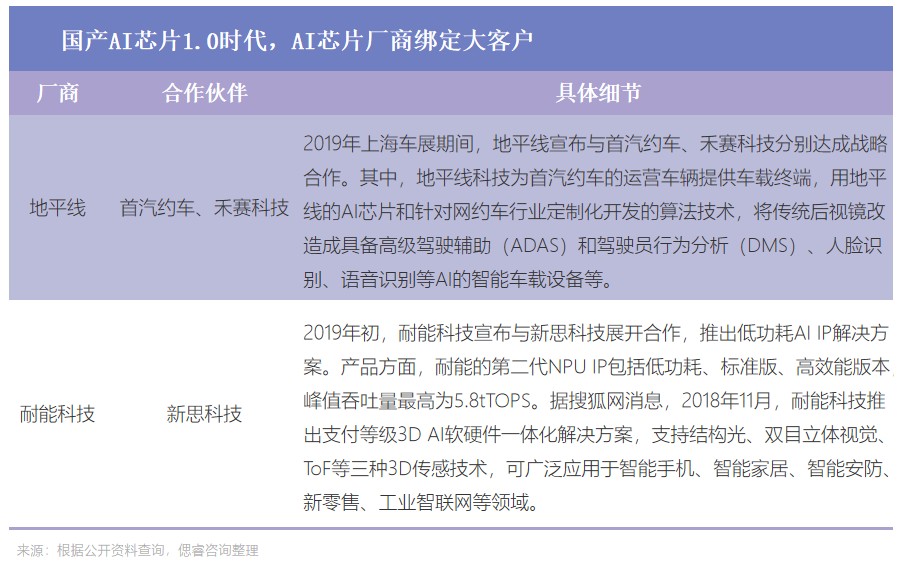
On the occasion of the coordinated development of large customers by Chinese factories, Ali, a big manufacturer with its own ecology, set up Pingtou Ge, a wholly-owned chip company, focusing on AI and quantum computing.
In 2019, the first AI chip released by Pingtou Ge, Guang800, was built based on ASIC architecture and used for cloud reasoning. According to Ali, the computing power of a light-containing 800 is equivalent to 10 GPUs, the reasoning performance of the light-containing 800 reaches 78563 IPS, and the energy efficiency ratio is 500 IPS/w. Compared with traditional GPU computing power, the cost performance is improved by 100%.
In the era of 1.0, the newly born domestic chip manufacturers chose to bind large customers, and the big manufacturers with comprehensive ecology chose to study internally and jointly embark on the journey of exploring the computing power of AI chips.
Although ASIC has the ultimate computing power and energy efficiency, it also has some problems, such as limited application scenarios, dependence on self-built ecology, difficult customer migration, long learning curve and so on.
As a result, GPGPU (General Graphics Processor), which is more versatile, has become the latest development direction in the field of AI computing through continuous iteration and development, and has become the guider in the era of AI chip 2.0.
Since 2020, the GPGPU architecture represented by NVIDIA has started to have good performance. By comparing the flagship products of NVIDIA in recent three generations, it is found that the performance of FP16 tensor is doubled year by year, while the cost of computing power is decreasing.

As a result, many domestic manufacturers have laid out GPGPU chips, focusing on CUDA compatibility and testing the limits of AI computing chips. Since 2020, new forces such as Zhuhai Core Power, Bijie Technology, Muxi, Denglin Technology, Tianzhixin and Hanbo Semiconductor have gathered their strength. Everyone’s unanimous action is: self-research the architecture, follow the mainstream ecology, and cut into the marginal scene.

In the first two eras, domestic AI chip manufacturers are trying their best to conform to the trend of the times, follow the pace of international manufacturers one after another, and solve the challenge of AI computing chips by developing the latest chips.
The change we can see is that in the 2.0 era, domestic AI chip manufacturers woke up to their own consciousness and tried to develop their own architecture in order to make a breakthrough.
The weak versatility of ASIC chips is difficult to cope with the endless stream of downstream applications. GPGPU is limited by high power consumption and low utilization rate of computing power, and large models put forward unprecedented requirements for computing power: at present, the large computing power required by large models is at least 1000TOPS and above.
Take the GPT-3 pre-training language model released in 2020 as an example. It uses the most advanced NVIDIA A100 GPU in 2020, and its computing power is 624TOPS. In 2023, with the model iteration in the pre-training stage of the model, the demand for blowout in the visit stage is added, and the demand for chip computing power in the future model will be at least thousands.
For example, in the field of automatic driving, according to Caitong Securities Research Institute, the computing power of a single chip required for automatic driving will be at least 1000+TOPS in the future: in April 2021, NVIDIA has released a DRIVE Atlan chip with a computing power of 1000TOPS; This year, NVIDIA directly launched the chip Thor, reaching 2000TOPS.
As a result, the industry urgently needs new architecture, new technology, new materials and new packaging to break through the ceiling of computing power. In addition, the increasingly tense geographical relationship undoubtedly poses new challenges to AI computing chip manufacturers who are highly dependent on advanced manufacturing processes.
Under these big backgrounds, a group of start-up companies set up centrally from 2017 to 2021 chose to break away from the traditional von Neumann architecture and lay out new technologies such as integration of storage and calculation. The China AI Chip 3.0 era officially kicked off.
At present, the integration of deposit and calculation is on the rise:
In academic circles, the number of articles related to deposit/near deposit on ISSCC has increased rapidly: from 6 articles in 20 years to 19 articles in 23 years; Among them, the number of digital in-memory calculations has increased rapidly to four in 22 years after it was first put forward in 21 years.
In the production sector, the giants have laid out the integration of storage and calculation, and there are nearly a dozen start-ups betting on this architecture in China:
At the end of Tesla’s 2023 Investor Day trailer, Tesla’s dojo Supercomputing Center and Storage and Computing Integrated Chip appeared one after another; Earlier, Samsung and Ali Dharma Institute, including AMD, also laid out and launched related products early: Ali Dharma Institute said that compared with the traditional CPU computing system, the performance of the storage and calculation integrated chip was improved by more than 10 times, and the energy efficiency was improved by more than 300 times; Samsung said that compared with the GPU accelerator equipped with HBM only, the energy consumption of GPU accelerator equipped with HBM-PIM is reduced by about 2100GWh a year.
At present, more than ten domestic start-ups such as Yizhu Technology, Zhicun Technology, Pingxin Technology, and Jiutian Ruixin are betting on AI computing power by adopting the integrated architecture of storage and computing, among which Yizhu Technology and Qianxin Technology are biased towards large computing power scenarios such as data centers.

At this stage, the insiders said that the integration of memory and computing will be expected to become the third computing architecture after CPU and GPU architecture.
The basis of this formulation is that the integration of storage and calculation has the advantage of high energy efficiency ratio in theory, and it can bypass the blockade of advanced processes, giving consideration to greater versatility and higher cost performance, and there is huge room for the development of computing power.
On this basis, the new memory can help the storage and calculation integration to achieve the above advantages better. At present, the mature memories that can be used for storage and calculation are NOR FLASH, SRAM, DRAM, RRAM, MRAM and so on. In contrast, RRAM has the advantages of low power consumption, high calculation accuracy, high energy efficiency ratio and manufacturing compatibility with CMOS process:

At present, the new storage RRAM technology has landed: in the first half of 2022, Xinyuan Semiconductor, a domestic startup company, announced that the first RRAM 12-inch pilot production line in mainland China had officially completed the installation acceptance and reached mass production and commercialization in the industrial control field. According to Dr. Qiu Shengbang, CTO of Xinyuan Semiconductor, the yield of Xinyuan RRAM products has exceeded 93%.
With the mass production of new memory devices, the AI chip with integrated memory and computing has entered the AI power chip landing competition.
However, whether it is a traditional computing chip or a memory-computer integrated chip, a large number of computing tasks in non-AI accelerated computing fields, such as logic computing and video codec, often need to be handled when accelerating AI computing. With multi-modal becoming the general trend of the big model era, AI chips will need to process many kinds of data such as text, voice, image and video in the future.
In this regard, the start-up company Yizhu Technology is the first to propose a super-heterogeneous AI computing technology path integrating storage and computing. Yizhu’s imagination is that if the new memristor technology (RRAM), integrated memory architecture, Chiplet technology, 3D packaging and other technologies can be combined, more effective computing power will be realized, more parameters will be placed, higher energy efficiency ratio will be realized, and better software compatibility will be achieved, thus raising the development ceiling of AI computing power chips.
Standing at the door of the 3.0 era, the independent consciousness of domestic AI computing chip manufacturers broke out, in order to provide the possibility of overtaking China AI computing chips in corners.
The driving force for the development of the AI chip market generally comes from the following factors.
In February 2023, the central government issued a number of related reports and layout plans, emphasizing the mobilization of computing power in East-West Computing. At present, it has fallen behind: an integrated service platform for East-West Computing.

At the local government level, for example, in January, 2023, Chengdu issued a "calculation voucher", that is, the government’s calculation resources were shared with calculation intermediary service agencies, small and medium-sized scientific and technological enterprises, makers, scientific research institutions, universities, etc., effectively improving the utilization rate of calculation power; In March 2023, Beijing issued relevant opinions on accelerating the implementation of computing power, and accelerated the construction of infrastructure such as computing centers, computing power centers, industrial Internet, and Internet of Things.

Based on the relevant policy guidelines of the state and local governments, AI manufacturers have set up supercomputing/intelligent computing centers one after another. Different from the past, the first market-oriented operation mode of computing power was born this year, and the scale of computing power in intelligent computing centers has also achieved a qualitative leap: According to the Guide to Innovation and Development of Intelligent Computing Centers jointly issued by the State Information Center and relevant departments, more than 30 cities in China are currently building or proposing to build intelligent computing centers.


It can be seen that the policy on AI chips has moved from the planning stage of the 13th Five-Year Plan to the landing stage of the 14th Five-Year Plan: improving the research and development technology of AI chips and popularizing AI applications.

At the same time, all localities clearly stated that it is necessary to strengthen the layout of the AI chip industry. Among them, Zhejiang, Guangdong, Jiangsu and other provinces have put forward the specific development direction of artificial intelligence chips by 2025.

The integration of deposit and calculation is becoming a new opportunity for the innovation and development of Shenzhen’s computing industry chain, and it is actively landing.
On April 2, 2023, at the second China Industrial Chain Innovation and Development Summit, Yang Yuchao, vice president of School of Information Engineering, Peking University Research Institute, said that Shenzhen would solve the challenge of the integration of storage and calculation in industrial application from four aspects: advanced technology and packaging, innovative circuit and architecture, EDA tool chain, software and algorithm ecology.
In April this year, China Big Model officially broke out. In the future, the demand for AI big computing chips will only increase.

The existing big model is opening to the lion of NVIDIA A100 big computing chip:

Therefore, AI manufacturers, such as Shang Tang, are focusing on domestic AI computing chips: on April 10th, 2023, Shang Tang revealed that at present, the proportion of domestic AI chips used in Shang Tang has reached 10%. This will undoubtedly accelerate the growth of domestic AI chip manufacturers.
NVIDIA said that in the future, it will start from the GPU architecture and move towards "GPU+DPU super-heterogeneity": launching NVLink-C2C and supporting UCLe+ pellet +3D packaging; Thor "super-heterogeneous" chip 2000 t was launched;
AMD said that the breakthrough of hardware innovation will be more difficult in the future, and it will move towards "system-level innovation", that is, collaborative design from upstream and downstream links of the overall design to improve performance.
The whole artificial intelligence industry chain is basically divided into three levels: basic layer, technical layer and application layer:
The basic layer includes AI chip, smart sensor, cloud computing, etc. The technical layer includes machine learning, computer vision, natural language processing, etc. The application layer includes robots, drones, smart medical care, smart transportation, smart finance, smart home, smart education, smart security and so on.

As the foundation of the development of artificial intelligence industry, the basic layer provides data and computing power support for artificial intelligence, among which AI chip is the basis of computing power of artificial intelligence.
When AI industry is not mature, the current value of basic enterprises is the largest. In China artificial intelligence industry chain, the proportion of basic enterprises is 83%, that of technical enterprises is 5%, and that of application enterprises is 12%.

The foundation layer determines whether the building is stable, while the downstream application layer determines the height of the building. In the application layer, smart terminals such as intelligent robots and drones have unlimited potential, and there is a lot of gold to dig in smart cities, smart medical care and other fields. At present, the scale of China’s intelligent robot market continues to grow rapidly.
The data shows that the market size of intelligent robots in China increased from 44.8 billion yuan to 99.4 billion yuan in 2017-2021, with a compound annual growth rate of 22.05%. It is estimated that the market size will reach 130 billion yuan in 2023.

According to the statistics of China Xintong Institute, the market size of smart cities in China has kept increasing by more than 30% in recent years. In 2021, the market size reached 21.1 trillion yuan, and it is estimated that the market size will reach 28.6 trillion yuan in 2023.

Under the global digital and intelligent wave, the technology of the technical layer is constantly iterating: technologies such as autonomous driving, image recognition and calculation are being deeply applied in various fields; At the same time, the Internet of Things devices in the application layer are constantly enriched: industrial robots, AGV/AMR, smart phones, smart speakers, smart cameras and so on.
This will undoubtedly promote the rapid growth of the AI chip and technology market at the basic level. According to the consulting data, the global AI chip market will reach $96 billion in 2022 and is expected to reach $308.9 billion in 2027, with a compound annual growth rate of 23% from 2022 to 2027:

The domestic AI chip market is even hotter: according to the consulting data, the AI market in China will reach $31.9 billion in 2022, and it is expected to reach $115 billion in 2027, with a compound annual growth rate of 29.2% from 2022 to 2027.

With the increasing demand in the downstream security and automobile markets, and since 2019, the United States has continued to sanction domestic manufacturers. In 2021, the domestic AI chip track will usher in the wind. In this year, the capital competed to select the "potential dogs" belonging to the AI chip market in China, in order to grasp the right to speak in the future chip market. Although the investment fever has declined in 2022, the total amount still exceeds 10 billion yuan.

(Overall situation of financing of artificial intelligence chip industry in China from 2016 to 2023. Source: Prospective Economist APP)
By analyzing the investment rounds, it is found that the AI chip market is still in its infancy: at present, the financing rounds of the artificial intelligence chip industry are still in the early stage, and the amount of financing after the C round is small.

(Investment and financing rounds of artificial intelligence chip industry in China from 2016 to 2023. Source: Prospective Economist APP)
In terms of track segmentation, GPU is the most valuable track, and GPU players such as Moore Thread have raised more than 1 billion yuan and won the "MVP";

The number of track financing companies with integrated deposit and calculation is the largest, and seven players with integrated deposit and calculation, such as Yizhu Technology and Zhicun Technology, are favored by capital. It is worth noting that the four start-up companies under the deposit and calculation integrated track, Yizhu Technology, Zhicun Technology, Pingxin Technology and Houmo Intelligent, have obtained financing for two consecutive years.

At present, players in the 1.0 era, such as Cambrian and Pingtou Brother, have now become listed companies with high-quality AI computing chips; Unlisted AI computing chip companies emerging in the era of 2.0, such as Bijie Technology, Denglin Technology, and Tianzhixin, continue to exert their strength on the product side; In the 3.0 era, startups such as Qianxin Technology and Yizhu Technology are seeking breakthroughs in the architecture of deposit and calculation.


According to the insight of Rui Rui, at present, most AI chip companies lay out small computing scenarios on the edge and center, such as smart security, smart city, smart medical care and other application scenarios; Biqi Technology, Pingtou Brother and Yizhu Technology can cover the scenes with large calculation force on the edge and center; In a new batch of start-ups, Yizhu Technology has made a bold attempt to make a big computing scene with the integrated architecture of storage and computing.
Therefore, according to the classification of architecture and application scenarios, we present the following panorama of upstream manufacturers in AI computing chips:

ChatGPT’s popularity has triggered a huge wave in the AI industry, and domestic AI chips are welcoming the 3.0 era. In the 3.0 era when the big model was born, it is urgent to provide sufficient computing power for the AI big computing chip to make the increasingly heavy big model roll up quickly.
With the opening of the "meta-universe" era, GPT-4 and other large models are coming to the fore, and data traffic will usher in explosive growth. According to IDC forecast data, it is estimated that the global computing power scale will increase by more than 50% in the next five years, and the overall scale will reach 3300EFlops by 2025. In 2025, the number of Internet of Things devices in the world will exceed 40 billion, and the amount of data generated is close to 80ZB, and more than half of the data needs to be processed by the computing power of the terminal or the edge.

(Future growth of global computing power demand Source: china galaxy Securities Research Institute)

(The growth rate of global computing power obviously lags behind the growth of data volume. Source: china galaxy Securities Research Institute)
With the rapid increase of data volume, countries urgently need computing power to maintain the normal operation of data, and the battle for computing power among countries has officially started. In fact, it’s far more than just a battle for computing power. Behind this is the competition of national strength of various countries.
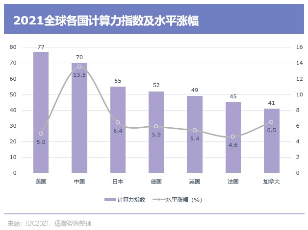
In March 2022, the Evaluation Report of Global Computing Power Index for 2021-2022, jointly compiled by IDC, Inspur Information and Tsinghua University Global Industry Research Institute, revealed the basic relationship between computing power and national strength:
There is a significant positive correlation between the scale of computing power and the level of economic development in countries around the world. The larger the scale of computing power, the higher the level of economic development. Every time the computing power index increases by 1 point on average, the digital economy and GDP will increase by 3.5‰ and 1.8 ‰ respectively; The computing power index of the United States and China is 77 and 70 respectively, which obviously highlights the computing power index of other countries.
From headphones, mobile phones and PCs to automobiles, Internet, artificial intelligence (AI), data centers, supercomputers and space rockets, "computing power" plays a fundamental and core role. Different computing scenarios have different requirements for the chip:

It can be seen that the data center has high requirements for the chip because of its diverse algorithms and faster iteration speed, such as high computing power, low power consumption, low cost, high reliability and higher versatility.
Among many application scenarios, data center is particularly important. As an AI infrastructure, the data center carries multiple applications of computing power on the center side and the edge side:
1. National data center cluster supports industrial Internet, financial securities, disaster warning, telemedicine, video calling and artificial intelligence reasoning.
2. As the "edge" end of computing power, the data center in the city serves high-frequency trading, VR/AR, ultra-high-definition video, car networking, networked drones, smart power, smart factories, intelligent security and so on in the financial market.
Nowadays, the battle for computing power and even national strength has already begun.
U.S. sanctions against China data center, intelligent computing center and supercomputing center began in 2021: In April 2021, the U.S. Department of Commerce listed China supercomputing entities such as Jinan Center, Shenzhen Center, Wuxi Center and Zhengzhou Center of China National Supercomputing Center.
Based on the demand growth in the downstream market, geopolitics and other factors, China’s data centers are also quickly put on the agenda: in May 2021, the state put forward the "East Counting and West Computing" project, clearly focusing on eight national computing hubs, and promoting the construction of national data center clusters and urban internal data centers.

Nowadays, there is still a certain gap between China’s data center construction and that of the United States:
According to the Global Computing Power Index Assessment Report 2021-2022, there are about 600 super-large data centers in the world, each with more than 5,000 servers, of which about 39% are in the United States, four times that of China, while the total number of servers in China, Japan, Britain, Germany and Australia accounts for about 30% of the total.

By the end of 2021, the total rack size of data center in use in China reached 5.2 million standard racks, the server size of data center in use was 19 million, and the total computing power scale exceeded 140 EFLOPS.
Under the background that computing power is national strength, under the catalysis of large model, large computing power with low cost and low power consumption will definitely become just needed. China is in urgent need of an autonomous and controllable data center capable of carrying computing power, and the computing power of the data center depends on the progress of domestic replacement of chips.
In the data center infrastructure, servers account for 69%. Nowadays, in the accelerated server market of data center, GPGPU is dominant by virtue of its higher performance and versatility:
According to IDC data, in 2021, GPU/GPGPU servers will occupy the dominant position in China’s accelerated server market with a share of 91.9%; The non-GPU acceleration servers such as ASIC and FPGA mentioned earlier only account for 8.1%.

At this stage, in the scene of cloud data center, there is still a gap between domestic GPGPU chips and internationally renowned ones.
Before the comparison, we need to be clear that in the cloud (server), the requirements for training chips and reasoning chips are not exactly the same:
The training chip needs to train a complex neural network model through massive data to adapt it to specific functions. Accordingly, it has high requirements for performance and accuracy, and it needs to be universal.
The inference chip uses neural network model for inference and prediction, which has lower requirements for peak calculation performance and pays more attention to comprehensive indicators such as unit energy consumption, time delay and cost.

At present, players such as Bibo Technology, Pingtou Ge, Kunlun Core, Muxi and Tianzhixin all have layouts for cloud data centers, among which most manufacturers such as Kunlun Core and Pingtou Ge have introduced reasoning chips; CAMBRIAN, Muxi, and Tianzhi Zhixin launched an integrated chip for training and pushing.
In recent years, domestic manufacturers have made breakthroughs in hardware performance of training chip products, but there is still a certain gap with mainstream NVIDIA A100 products in the market:

Take Suihara Yunjia T20 product as an example, its 32-bit single-precision floating-point performance reaches 32TFLOPS, which is higher than A100′ s 19.5TFLOPS, and it has more advantages in power consumption, but the memory bandwidth is less than 1/3 of A100′ s, so there is still a gap in meeting the bandwidth requirements of machine learning and deep learning.
At the same time, according to the analysis of Zheshang Securities, Siyuan 590 series launched at the end of Cambrian last year may show better performance in some models because of its ASIC specificity, but due to its lack of versatility, it still needs post-adaptation and technical support. In contrast, there is still a certain gap between China AI training chip and NVIDIA in performance and ecology (compatibility).

At present, the products of domestic manufacturers such as CAMBRIAN, Suiyuan and Kunlun Core have the ability to compete with Tesla T4, which is the mainstream in the market. Its energy efficiency ratio is 1.71TOPS/W, which is smaller than T4′ s 1.86 tops/w..
The gap is still there, and domestic AI manufacturers need to catch up with the international speed. The first step to improve the performance of the chip is to roll up the advanced process.
At present, the design cost of advanced process chips is high: the cost per unit area increases sharply after 14/16nm.

(The cost per unit area of advanced process chips increases. Source: TF Securities)
1. According to the singular molar data, with the evolution of the process from 28nm to 5nm, the R&D investment has also increased sharply from 51.3 million US dollars to 542 million US dollars, and the development cost of 2nm is close to 2 billion US dollars. The advanced process has become a money-burning competition for global giants.
2. According to WeChat official account data of EETOP, the cost of designing a chip at 7nm node is as high as 300 million dollars. And with Moore’s law slowing down, transistors approach the physical limit and the cost limit at the same time.
As a result, chip upstream enterprises are also frantically raising prices: the price of advanced process wafers of supplier TSMC is rising every year, and the more it rises, the more outrageous it is.

3. Previously, the price was increased by processes: In 2021, TSMC informed customers to increase the price in an all-round way at noon on August 25th. From now on, the advanced processes of 7nm and 5nm will increase the price by 7% to 9%, and the prices of other mature processes will increase by about 20%;
4. At the beginning of 2023, the price of TSMC rose sharply across the board: According to the Electronic Times, the price of TSMC’s 12-inch 5nm wafer was as high as $16,000 per wafer, which was 60% higher than that of the previous generation 7nm wafer.
The rising cost will become the norm. What’s more regrettable is that the performance has not surpassed that of NVIDIA even though domestic manufacturers have rolled up the manufacturing process to 7nm.

If it is rolled to 5nm to achieve higher performance, chip manufacturers will lose more than they gain:
First of all, the cost is unaffordable. NVIDIA’s moat in GPGPU was smashed out by money. According to NVIDIA Huang Renxun, the research and development cost of A100 chip alone is $2-3 billion (at the level of 10 billion yuan) and four years. In the short term, domestic start-ups do not have such a large volume and cannot afford the time cost.

At present, the high R&D cost has made Cambrian and other manufacturers still unprofitable.

Secondly, the money has been spent, which has no effect: the performance is not maintaining "positive growth". Logic chips are still evolving along Moore’s Law, and memory chips continue to shrink in size, which no longer has the advantages in cost and performance. On the contrary, the reduction of analog chip manufacturing process may lead to the decline of analog circuit performance.

At the same time, in the long run, 7nm chips are more cost-effective than 5nm chips:
Georgetown University published an AI chip research report, in which the economic benefits of AI chips with different process nodes were analyzed. The report reveals through the quantitative model that the cost-benefit of 7nm process chip is better than that of 5nm process node.

Researchers have drawn two conclusions from this cost analysis model:
1. Within two years of normal operation, the energy consumption cost of chips with advanced technology (7/5nm) exceeded its production cost, and the energy consumption cost of chips with old technology (10nm and above) increased faster. If the production cost and operation cost are considered comprehensively, the cost benefit of advanced process chips is 33 times that of old process chips.
2. Comparing the 7nm and 5nm chips, when they are used in normal operation for 8.8 years, the cost of the two chips is equivalent. This means that 7nm is more cost-effective if the chip is replaced within 8.8 years. In view of the fact that the AI accelerators used in AI training and reasoning in data centers are mostly replaced once every three years, 7nm chips are more cost-effective than 5nm chips in terms of cost-effectiveness.
In addition, there is geopolitical influence, and domestic advanced process research and development has been repeatedly blocked. The chip has suffered from the advanced manufacturing process for a long time, and improving the computing power of the chip is not only to improve the performance of a single chip, but also to consider the macro-finishing power of the chip.
Macro-force = performance * quantity (scale) * utilization, but at present, what we can see is that many schemes can’t take these three factors into account:
1. Some computing chips can achieve soaring performance, but less consideration is given to the versatility and ease of use of the chips, resulting in low chip sales and small landing scale. For example, customization through FPGA means that the scale is too small and the cost and power consumption are too high.
2. Some computing power improvement schemes focus on scale investment, but they can’t solve the fundamental problem of future computing power demand order of magnitude improvement.
3. Some solutions improve the utilization rate of computing power by pooling various resources and sharing computing power across different boundaries, but they cannot change the essence of the current performance bottleneck of computing chips.
In order to achieve great computing power, it is necessary to take into account the three major influencing factors of performance, scale and utilization rate, and have a comprehensive plan.
Taking the AI cloud reasoning card as an example, we can see that from 2018 to 2023, due to various reasons such as "the process is not moving", it is difficult to balance the cost, power consumption and computing power.
However, the battle for national strength has started, ChatGPT has arrived, and the market urgently needs a solution that takes into account cost, power consumption and computing power.
At present, international manufacturers, domestic mainstream manufacturers and start-ups are all seeking innovation in computing architecture, trying to find a solution that takes into account performance, scale and utilization, and break through the ceiling of computing power.

For architecture innovation, there are many technologies and schemes in the industry: quantum computing (quantum chip), photonic chip, memory and computation integration, Chiplet, 3D packaging, HBM …

Among them, HBM, pellets, 3D packaging and storage are now compatible with CMOS technology and can be mass-produced as soon as possible. The integration of storage and computation and Chiplet are two clear routes that are generally believed in the industry to break through the AI computing dilemma and carry out architectural innovation.
From the traditional von Neumann architecture to the integrated architecture of storage and calculation, in general, it is to eliminate the gap between data and make it work more efficiently.
Under the traditional von Neumann architecture, the storage and computing areas of the chip are separated. When computing, data needs to be transported back and forth between two areas. With the increasing number of layers and scale of neural network model and data processing capacity, data has already faced the situation of "running over", which has become the bottleneck of high-performance computing performance and power consumption, which is also commonly known as the "storage wall" in the industry.
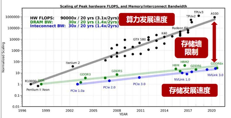
(The specific performance of storage wall restrictions Source: Zheshang Securities)
The storage wall also brings the problems of energy consumption wall and compilation wall (ecological wall). For example, the problem of compilation wall is that a large amount of data handling is prone to congestion, and the compiler can’t optimize operators, functions, programs or networks as a whole under static and predictable conditions, but can only optimize programs manually, one by one or layer by layer, which consumes a lot of time.
These "three walls" will lead to unnecessary waste of computing power: according to statistics, in AI applications with large computing power, data handling operations consume 90% of time and power consumption, and the power consumption of data handling is 650 times that of operation.
The integration of storage and calculation can integrate storage and calculation, completely eliminate the delay of memory access and greatly reduce power consumption. Based on this, Zheshang Securities reported that the advantages of the integration of deposit and calculation include but are not limited to: greater computing power (above 1000TOPS), higher energy efficiency (over 10-100TOPS/W), cost reduction and efficiency increase (which can exceed one order of magnitude) …
As shown in the following figure, compared with GPGPU, the integrated memory and computing chip can achieve lower energy consumption and higher energy efficiency ratio, and can help data centers reduce costs and increase efficiency in application landing, empowering green computing power.

Based on this, the initial investment of the integrated storage and calculation chip is 13%-26% of A100, and the daily electricity bill is 12% of A100.

In addition to breaking the wall between data, chip designers try to give chips more capabilities: distribute tasks to hardware computing units with different architectures (such as CPU, GPU, FPGA), so that they can do their own jobs, work synchronously and improve efficiency.
Looking back at the history of computer development, AI chip processors are from single-core to multi-core, and computing is from serial to parallel, from isomorphic parallel to heterogeneous parallel.

When Moore’s law was the iron law of the industry, that is, the first stage, computer programming was almost always serial. Most programs only have one process or thread.
At this point, the performance depends on the hardware process. After 2003, because the process has reached the bottleneck, it is not feasible to rely solely on hardware upgrade. Then, even if the isomorphic computing was ushered in (overlapping multiple cores and forcibly improving the computing power), the overall ceiling still existed.
The arrival of heterogeneous parallel computing has opened up a new technological change: tasks are distributed to hardware computing units with different architectures (such as CPU, GPU and FPGA), so that they can do their own jobs, work synchronously and improve efficiency.
Benefits of Heterogeneity: From the software point of view, heterogeneous parallel computing framework can enable software developers to develop heterogeneous parallel programs efficiently and make full use of computing platform resources.
From the hardware point of view, on the one hand, many different types of computing units improve their computing power through more clock frequencies and the number of cores; On the other hand, various computing units improve their execution efficiency through technical optimization.
Among them, Chiplet is the key technology.

Under the current technological progress, Chiplet scheme can reduce the complexity and cost of chip design. In the IC design stage, the SoC is decomposed into multiple cores according to different functional modules, and some cores are modularized and reused in different chips, which can reduce the design difficulty, facilitate the subsequent product iteration and accelerate the product launch cycle.
Due to the development of semiconductor industry and the difference of demand, the processor and the memory go to different process routes, which means that the process, packaging and demand of the processor and the memory are very different.
As a result, the performance gap between them has been increasing since 1980. The data shows that from 1980 to 2000, the speed mismatch between processor and memory increased at a rate of 50% per year.

(From 1980 to 2000, the speed mismatch between the processor and the memory increased by 50% every year. Source: Electronic Engineering Album)
The data access speed of memory can’t keep up with the data processing speed of processor, and the narrow data exchange path between them and the high energy consumption caused by it have built a "memory wall" between storage and operation.
In order to reduce the influence of memory wall, improving memory bandwidth has always been a technical issue concerned by memory chips. Huang Renxun once said that the biggest weakness of computing performance expansion is memory bandwidth.
HBM is the solution to this difficult problem.
High Bandwidth Memory is a kind of hardware storage medium. Because of its high throughput and high bandwidth, it has attracted the attention of industry and academia.
One of the advantages of HBM is to shorten the distance between the memory and the processor through the intermediary layer, and to package the memory and the computing unit together through the advanced 3D packaging method to improve the data handling speed.
Super-heterogeneous computing is a computing that can integrate and reconstruct more heterogeneous computing, so that all types of processors can fully and flexibly interact with each other.
To put it simply, it is to aggregate the advantages of DSA, GPU, CPU, CIM and other types of engines, and at the same time combine the emerging architectures such as Chiplet and 3D packaging to achieve a leap in performance:
√ DSA is responsible for the relatively determined work with a large amount of calculation;
√ GPU is responsible for some performance-sensitive and flexible work in the application layer;
√ CPU can do anything and is responsible for the bottom;
√ CIM is in-memory computing. The main difference between super-heterogeneous and ordinary heterogeneous is that CIM is added, which can achieve the same computing power and lower energy consumption; The same energy consumption, higher computing power. In addition, CIM can bear more computing power than DSA because of the advantages of devices.
Hyperheterogeneous computing can solve the problems of performance, scale and utilization.
On the performance level, due to the integration of storage and calculation, it can achieve the same computing power and lower energy consumption; The same energy consumption, higher computing power;
On the scale level, because hyperheterogeneity can aggregate multiple types of engines based on a computing platform, it can give consideration to flexibility and versatility, so there is no small scale because it is not universal enough; Because the scheme is versatile, it can cope with all kinds of tasks, and the utilization rate can also be improved.
However, the reality is that only heterogeneous computing is faced with the dilemma of programming. After several years of efforts, NVIDIA has made CUDA’s programming friendly enough for developers and formed a mainstream ecology.
Super-heterogeneity is even more difficult: the difficulty of super-heterogeneity is not only reflected in programming, but also in the design and implementation of processing engine, and also in the integration of software and hardware capabilities of the whole system.
For better control of super-heterogeneity, the integration of software and hardware gives the direction:
1. Give consideration to performance and flexibility. From the system point of view, the task of the system is accelerating from CPU to hardware. How to choose the appropriate processing engine to achieve optimal performance and flexibility. And it is not only a balance, but also a consideration.
2. Programming and ease of use. The system gradually changed from hardware-defined software to software-defined hardware. How to use these features, how to use existing software resources, and how to integrate into cloud services.
3. products. User needs, in addition to the demand itself, also need to consider the differences of different user needs, and the long-term iteration of individual user needs. How to provide users with better products and meet the short-term and long-term needs of different users. It is better to teach people to fish than to teach people to fish. How to provide users with a fully programmable hardware platform with extreme performance without specific specific functions?
Computing power is national strength, and data centers are the "base areas" for countries to carry out national strength disputes. The data center is in urgent need of large computing chips to meet the needs of application scenarios at the center and edge.
However, in the data center application scenario, there is still a big gap between the existing domestic cloud AI training and reasoning chip and the top student NVIDIA A100 chip. At the same time, at present, the technological process has reached the physical limit and cost limit, so seeking a more efficient computing architecture is the best choice.
Nowadays, technologies such as integration of storage and computing, Chiplet and 3D packaging are mature, and solutions such as super-heterogeneous are highly implementable. In the traditional architecture, the gap between countries is obvious, but in the new technology, countries are indistinguishable.
The pattern of the struggle for computing power is quietly changing.
According to the market structure, there are currently three types of players in the field of AI chips.
One is the old chip giants represented by Nvidia and AMD, which have accumulated rich experience and outstanding product performance. According to the above, in the cloud scene, domestic manufacturers have a gap with both reasoning chips and training chips.
The other is the cloud computing giants represented by Google, Baidu and Huawei. These enterprises have laid out general big models and developed their own AI chips and deep learning platforms to support the development of big models. Such as TensorFlow and TPU from Google, Kunpeng and Shengteng from Huawei, and Guangguang 800 from Ali Pingtou.
Finally, the unicorn of AI chip, such as CAMBRIAN, Bijie Technology, Horizon, etc., broke into the AI chip track with strong technical strength, capital base and R&D team.
At present, Nvidia occupies more than 80% of China’s accelerator card market share, and domestic AI chips need to be developed urgently: according to IDC data, the number of China accelerator cards shipped in 2021 has exceeded 800,000, of which NVIDIA occupies more than 80% of the market share. The remaining share is occupied by brands such as AMD, Baidu, Cambrian, Suiyuan Technology, Xinhua III and Huawei.
According to the classification of computing architecture, at present, China is divided into three camps: ASIC, GPGPU, and integrated storage and computing players.
By combing the use architecture, application scenarios and resource endowments of various vendors, we can find the following clues:
Domestic manufacturers Huawei Hisilicon, Baidu and Pingtou Ge all chose ASIC as their chip architecture:
1. Huawei chooses to deploy an end-to-end complete ecosystem. For example, the use of Ascension 910 must be matched with Huawei’s big model support framework MindSpore and Pangu Big Model.
2. Ali is positioned as a system integrator and service provider in this respect, using its own chip products to build an acceleration platform and export services to the outside world.
3. Baidu Kunlun Core is mainly used in its own intelligent computing clusters and servers, as well as domestic enterprises, research institutes and governments.
Although ASIC is highly integrated, its performance can be fully exerted and its power consumption can be well controlled, its shortcomings are also obvious: limited application scenarios, dependence on self-built ecology, difficulty in customer migration, long learning curve and so on.
However, large factories have multiple specific scenarios, and the disadvantages of ASIC "limited application scenarios and difficult customer migration" no longer exist in large factory scenarios. At the same time, it is significantly less difficult to choose ASIC in mass production and manufacturing supply chain than GPU.
AI chip manufacturers that focus on autonomous driving scenarios, such as Horizon and Black Sesame, have also avoided the disadvantages of ASIC because they hold many orders: as of April 23, 2023, the shipment of Horizon Journey chips exceeded 3 million pieces, and they reached fixed-point cooperation with more than 20 car companies, totaling more than 120 models.
Because ASIC can only exert its extreme performance under specific scenarios and inherent algorithms, manufacturers need to have their own specific scenarios (such as Huawei and other big manufacturers) or bind large customers (such as Naineng Technology). The more general GPGPU has become the first choice for domestic AI chip companies after showing its due performance.
It can be seen that boarding technology, Tianxin Zhixin and Suiyuan technology, which choose GPGPU, have fully covered training and reasoning, while most ASIC chips, such as Pingtou Brother, can only focus on reasoning or training scenarios.
Before and after the development of AI computing chips in 2019, domestic AI chip manufacturers found that under the traditional architecture, CPU, GPU and FPGA have been monopolized by foreign countries, and domestic AI manufacturers, which are highly dependent on advanced process technology and lack of advanced process technology reserves, are looking for new solutions-storage and calculation integrated chips. At present, the pattern of integration of deposit and calculation has not been decided, or it will become the key for domestic manufacturers to break the game. According to the distance between the computing unit and the storage unit, the main stream of storage and calculation can be roughly divided into near storage calculation (PNM), storage processing (PIM) and storage calculation (CIM).

Tesla, Ali Dharma Institute, Samsung and other big companies have chosen near-memory computing.
According to Ganesh Venkataramanan, director of Dojo project, compared with other chips in the industry, the D1 chip used in Tesla Dojo(AI training computer) has improved performance by 4 times at the same cost, improved performance by 1.3 times at the same energy consumption and saved space by 5 times. Specifically, in terms of D1 training modules, each D1 training module is arranged by 5×5 D1 chip array and interconnected in a two-dimensional Mesh structure. On-chip cross-core SRAM reaches an astonishing 11GB, and the energy efficiency ratio is 0.6TFLOPS/W@BF16/CFP8 due to the use of near memory computing architecture. According to industry insiders, this energy efficiency ratio is very good for CPU architecture.
In 2021, Ali Dharma Institute released the 3D stacking technology using Hybrid Bonding, which connects the computing chip and the memory chip face-to-face with specific metal materials and processes. According to the calculation of Ali Dharma Institute, in the practical recommendation system application, compared with the traditional CPU computing system, the performance of the integrated storage and calculation chip is improved by more than 10 times, and the energy efficiency is improved by more than 300 times.
Based on the in-memory processing architecture, Samsung released the memory product HBM-PIM (PNM in a strict sense). Samsung said that the architecture achieved higher performance and lower energy consumption: compared with other GPU accelerators without HBM-PIM chip, HBM-PIM chip doubled the performance of AMD GPU accelerator card and reduced the energy consumption by about 50% on average. Compared with GPU accelerator equipped with HBM only, the energy consumption of GPU accelerator equipped with HBM-PIM is reduced by about 2100GWh a year.
Domestic Zhicun Technology chose in-memory processing: In March 2022, Zhicun Technology’s mass-produced PIM-based SoC chip WTM2101 was officially put into the market. Less than a year ago, WTM2101 has been successfully commercialized on the end side, providing AI processing solutions such as voice and video and helping products achieve more than 10 times energy efficiency improvement.
And in-memory computing is what most domestic start-ups call the integration of storage and computing:
Yizhu Technology, based on CIM framework and RRAM storage medium, develops a "all-digital storage and calculation integrated" large computing power chip, which improves the energy efficiency ratio of operation by reducing data handling, and at the same time ensures the accuracy of operation by using the digital storage and calculation integrated method, which is suitable for cloud AI reasoning and edge calculation.
Zhixin Kewei launched the industry’s first edge-side AI enhanced image processor based on SRAM CIM at the end of 2022.
In the camp of integration of deposit and calculation, big factories and start-ups have also taken different paths because of the technical path.
Large companies and start-ups are "consciously" divided into two camps: Tesla, Samsung, Alibaba and other large companies with rich ecology, as well as traditional chip manufacturers such as Intel and IBM, almost all of which are laying out PNM;; And start-ups such as Zhicun Technology, Yizhu Technology, and Zhixinke are betting on PIM, CIM, etc., which are more intimate in saving and calculating.
What the comprehensive ecological factory considers is how to quickly break through the bottleneck of computing power and power consumption and let its rich application scenarios land quickly; Chip manufacturers have developed technologies that meet customers’ demands for high computing power and low power consumption.
In other words, the demand for the integrated architecture of storage and computing put forward by large factories is "practical and fast", and near-storage computing, as the technology closest to the project landing, has become the first choice of large factories.
However, China start-ups lack advanced 2.5D and 3D packaging capacity and technology due to their short establishment time and weak technical reserves. In order to break the US technology monopoly, China start-ups focus on CIM without considering advanced process technology.
Different business scenarios have shown their own advantages, and the business model is in the exploration stage at home and abroad. Regardless of domestic and foreign companies, cloud reasoning is the consistent direction of everyone.
The industry generally believes that it is more difficult to develop and commercialize training chips. Training chips can do reasoning, but reasoning chips can’t do training.
The reason is that the neural network model is not fixed in the process of AI training, so there is a high demand for the versatility of the chip. The reasoning is simpler and the growth rate is faster, so the training chip has a higher test for the design ability of the chip company.
Judging from the global AI chip market, reasoning before training is the mainstream path, as are Habana, an AI chip company acquired by Intel, and many domestic AI startups.
This choice is also the catalytic effect of the downstream market:
With the gradual maturity of AI model training in recent years, AI applications have gradually landed, and the market of cloud reasoning has gradually surpassed the training market:
According to the Evaluation Report on the Development of Artificial Intelligence Computing Power in China from 2020 to 2021 jointly issued by IDC and Inspur, the reasoning load of AI servers in China market will exceed the training load in 2021, and with the application of AI, the compound growth rate of reasoning computing power demand in data centers will be more than twice that of the training side, and it is estimated that the proportion of accelerators used for reasoning will exceed 60% by 2026.

After 2019, most of the newly-added AI chip manufacturers are integrated in storage and calculation: according to incomplete statistics of Zhai Rui’s insight, there are 20 newly-added AI chip manufacturers in 2019-2021, among which 10 choose the integrated storage and calculation route.
All these indicate that the integration of storage and calculation will become a rising star in Ran Ran after GPGPU, ASIC and other architectures. And this new star, not everyone can pick it.
In the situation that academic circles, production circles and capital are all optimistic about the integration of deposit and calculation, strong technical strength, solid talent reserve and accurate control of the acceptance of migration costs are the key to maintaining the competitiveness of start-ups in the industry, and they are also the three thresholds in front of new players.
The integration of storage and calculation has broken three walls and can achieve low power consumption, high computing power and high energy efficiency ratio. However, there are many challenges to achieve such performance:
First of all, the integration of storage and calculation involves the whole process of chip manufacturing: from the lowest device to circuit design, architecture design, tool chain, and then to the research and development of software layer;
Secondly, while making corresponding changes at each level, we should also consider the fitness between levels.
We look at it layer by layer, and what kind of technical problems are there when a memory-computing integrated chip is made.
First of all, in the choice of devices, manufacturers are "walking on thin ice": memory design determines the yield of chips, and once the direction is wrong, the chips may not be mass-produced.
Secondly, the circuit design level. With devices at the circuit level, it is necessary to use them for the circuit design of storage arrays. At present, in circuit design, in-memory calculation is not guided by EDA tools and needs to be done manually, which undoubtedly greatly increases the difficulty of operation.
Then, after there is a circuit at the architecture level, it is necessary to design the architecture level. Each circuit is a basic computing module, and the whole architecture is composed of different modules. The design of the integrated memory and computing module determines the energy efficiency ratio of the chip. The analog circuit will be disturbed by noise, and the chip will encounter many problems when it runs after being affected by noise.
In this case, it is necessary for architects to understand the process characteristics of simulated in-memory computing, design the architecture according to these characteristics, and also consider the adaptability between the architecture and software development.
After the software architecture design is completed, the corresponding tool chain needs to be developed.

However, because the original model of storage and calculation integration is different from the model under the traditional architecture, the compiler should adapt to the completely different storage and calculation integration architecture to ensure that all computing units can be mapped to the hardware and run smoothly.
A complete technical chain will test the ability of devices, circuit design, architecture design, tool chain and software layer development, and coordinate the adaptability of each link, which is a protracted war that consumes time, effort and money.
According to the operation flow of the above links, it can be seen that the integrated memory and computing chip urgently needs experienced circuit designers and chip architects.
In addition, in view of the particularity of the integration of deposit and calculation, a company that can make the integration of deposit and calculation needs to have the following two characteristics in personnel reserve:
1, leaders need to have enough courage. There should be a clear idea in the choice of devices (RRAM, SRAM, etc.) and calculation modes (traditional von Neumann, integrated storage and calculation, etc.).
This is because, as a subversive and innovative technology, the integration of storage and calculation has no leader and the cost of trial and error is extremely high. The founders of enterprises that can realize commercialization often have rich experience and academic background in industry and large factories, and can lead the team to complete product iteration quickly.
2. In the core team, it is necessary to equip experienced talents at all levels of technology. Such as the architect, who is the core of the team. Architects need to have a deep understanding and cognition of the underlying hardware and software tools, and can realize the envisaged storage architecture through technology, and finally achieve the product landing;
3. In addition, according to the qubit report, there is a lack of high-end talents in circuit design in China, especially in the field of hybrid circuits. In-memory computing involves a lot of analog circuit design. Compared with digital circuit design that emphasizes teamwork, analog circuit design needs personal designers who are extremely familiar with technology, design, layout, model pdk and packaging.
Landing is the primary productive force. At the time of delivery, customers consider not only the integrated storage and computing technology, but whether the performance indicators such as energy efficiency ratio, area efficiency ratio and ease of use of the integrated storage and computing SoC have been sufficiently improved compared with previous products, and more importantly, whether the migration cost is within the tolerance range.
If choosing a new chip to improve the performance of the algorithm requires re-learning a programming system, and the labor cost spent on model migration is higher than the cost of buying a new GPU, then customers will not choose to use a new chip with a high probability.
Therefore, whether the integration of storage and calculation can minimize the migration cost during the landing process is a key factor for customers when choosing products.
At present, NVIDIA has occupied the market of China AI accelerator card with the more general GPGPU.
However, with its low power consumption but high energy efficiency ratio, the memory-computing integrated chip is becoming a rising star in Ran Ran.
However, the market of deposit and calculation is still in the stage of "Xiao He just shows his sharp corner". However, we can’t deny that players with integrated storage and calculation have built three high walls. Those with strong non-technical strength and solid talent reserves are not allowed to enter.
With the rise of big data applications such as artificial intelligence, the integration of storage and calculation technology has been widely studied and applied by academic and industrial circles at home and abroad. At the 2017 Annual Meeting of Microprocessors (Micro 2017), NVIDIA, Intel, Microsoft, Samsung, University of California, Santa Barbara, etc. all launched their prototypes of integrated memory and computing systems.
Since then, the number of articles related to deposit/near deposit on ISSCC has increased rapidly: from 6 articles in 20 years to 19 articles in 23 years; Among them, digital in-memory calculation, which was first put forward in 21 years, increased rapidly to 4 in 22 years and 6 in 23 years.

(ISSCC2023 related articles on deposit and calculation integration Source: ISSCC2023)
System-level innovation is frequently appearing in semiconductor top-level conferences, showing the potential to break the ceiling of computing power.
In the keynote speech "Innovation for the Next Decade of Computing Efficiency" by Lisa Su (lisa su), president and CEO of AMD, she mentioned the rapid development of AI application and the demand it brings to chips.
According to Lisa Su, according to the current law that the computing efficiency is increased by 2.2 times every two years, it is estimated that by 2035, if the computing power is to reach 10 trillion, the power required will reach 500MW, which is equivalent to the power generated by half a nuclear power plant. "This is extremely outrageous and unrealistic."
In order to achieve such efficiency improvement, system-level innovation is one of the most critical ideas.

(Relationship between Computing Power and Power Consumption Source: ISSCC2023 Conference)
In another keynote speech brought by IMEC/CEA Leti/Fraunhofer, the three most famous semiconductor research institutions in Europe, system-level innovation is also its core keyword.
The speech mentioned that with the semiconductor technology approaching the physical limit, the demand for chips in new applications must be considered from the system level, and mentioned that the next generation smart car and AI are two core applications that especially need chip innovation from the system level to support their new requirements.
System-level innovation is a collaborative design of multiple links in the upper, middle and lower reaches to achieve performance improvement. There is also a saying that the system process is cooperatively optimized.
Collaborative optimization of system process is an "outside-in" development model, starting from the workload and its software that the product needs to support, to the system architecture, to the chip types that must be included in the package, and finally to the semiconductor process technology.

(System Process Collaborative Optimization Source: ISSCC2023 Conference)
Simply put, it is to optimize all the links together, so as to improve the final product as much as possible.
In this regard, Lisa Su gave a classic case: while using innovative number system (such as 8-bit floating-point number FP8) on the model algorithm level, optimizing and supporting the algorithm level at the circuit level, and finally improving the efficiency of the computing level by an order of magnitude: compared with the traditional 32-bit floating-point number (FP32), FP8 with system-level innovation can improve the computing efficiency by as much as 30 times. However, if we only optimize the efficiency of the FP32 computing unit, it is difficult to achieve an order of magnitude of efficiency improvement in any case.

(Domain-specific computing supports workload optimization to improve performance and efficiency. Source: ISSCC2023 Conference)
This is the reason why system-level innovation has become the key path: if the circuit design only stays at the circuit level-just considering how to further optimize the efficiency of FP32 computing unit, it is difficult to achieve an order of magnitude efficiency improvement in any case.
In this regard, in the speech of the future development opportunity module, Lisa Su gave a general picture of the future system-level packaging architecture: including heterogeneous computing clusters, specific acceleration units, advanced packaging technology, high-speed inter-chip UCIe interconnection, memory and computing integration and other memory technologies.

(Future System-in-Package Architecture Source: ISSCC2023 Conference)
The technical path and scheme are already clear, and the next step is the stage of hard work.
Every R&D manufacturer of emerging technologies will undoubtedly face problems at all levels in the early stage, such as technical exploration hitting a wall and downstream manufacturers disagreeing. In the early days, whoever first predicts the future development trend and uses it to take the step of exploration and lay down reasonable resources to try will seize the opportunity.
Chip giant NVIDIA has set a good example in this regard.
When the wave of data center has not been overwhelming, and artificial intelligence training is still a niche field, NVIDIA has invested heavily in developing general computing GPU and unified programming software CUDA to find a good job for NVIDIA-computing platform.
At that time, it was "useless and losing money" to make GPU programmable: I don’t know whether its performance can be doubled, but product development will be doubled. For this reason, no customer is willing to pay for it. However, it is not a long-term solution to predict a single-function graphics processor. NVIDIA resolutely decided to apply CUDA to all product lines.
In an interview with Dr. Lai Junjie, Senior Director of Engineering and Solutions in China District, NVIDIA, Lai Junjie said: "For the vision of computing platform, Huang Renxun quickly mobilized a lot of resources up and down in NVIDIA."
Foresight+heavy investment, in 2012, NVIDIA was rewarded by the innovator: In 2012, the computing performance of deep learning algorithm caused a sensation in academic circles. As a productivity tool with high computing power, GPU+CUDA quickly became popular in computer science and became the "standard" for artificial intelligence development.
Nowadays, the integration of storage and calculation has shown strong performance, and it has outstanding performance in artificial intelligence neural network, multi-modal artificial intelligence calculation, brain like computing and other large computing scenes.
Domestic manufacturers have also laid out the integration of storage and computing around 2019, and at the same time, they have chosen emerging technologies such as 3D packaging and chiplet, and emerging memories such as RRAM and SRAM to break through the ceiling of computing power.
In the war of AI computing chips, innovators are the first.
ChatGPT’s hot attack has triggered a huge wave in the AI industry, and domestic AI chips are welcoming the 3.0 era; In the era of 3.0, the chip architecture that is more suitable for the big model-the integration of storage and calculation will emerge, and system-level innovation will become the future development trend, and the manufacturers who bet first will get the bonus brought by ChatGPT first.
This article is published by Entrepreneurial State authorized by the columnist, and the copyright belongs to the original author. The article is the author’s personal opinion and does not represent the position of the entrepreneurial state. Please contact the original author for reprinting. If you have any questions, please contact editor@cyzone.cn.